CPLD & FPGA Programming - JTAG ISP
OEM product development teams are using more programmable logic (FPGAs and CPLDs) in their systems than ever before to help minimize their engineering risks and shorten the time it takes to bring new products to market. Configuring these FPGAs is normally handled through the use of special electrically alterable configuration PROMs, serial EEPROMs or with SRAMs that load the FPGAs with their designs at system power-up.
EclipseTM Test Development Environment can be used to rapidly configure IEEE 1532 compliant devices in-system. Configuring devices in-system reduces part costs, eliminates the need to stock pre-configured devices in inventory and enables field upgrades.
 In-System Programming with Eclipse
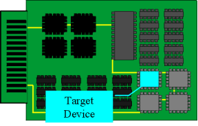
To configure a device in-system
Eclipse uses a file that contains the bitstream of FPGA and CPLD
configuration data. This file is generated from the device design
tools.
Eclipse accepts vector files from the most widely
used CPLD and FPGA vendors including: Xilinx, Altera, Actel, AMD,
Cypress and Lattice.
The first step for in-system configuration is to open up an Eclipse Database that contains the FPGA or CPLD to be configured and adjust the UltraTAPTM Intelligent Test Controller to the
proper voltage level for the target scan-chain. Next, Eclipse
will perform a Scan Path Integrity Test (SPIT) to assure that the
JTAG 1149.1 test logic and scan-chain is functioning properly. In the event of a scan path
error, Eclipse will not apply the programming information so
the device will not be damaged because of the faulty
scan-chain. If the scan path is OK, Eclipse will then apply
and program the target device, adjusting the programming
data automatically for various scan-chain positions of the
target device. Dynamic scan-chains found in complex PCBs and
multi-PCB systems are handled automatically.
Intellitech has developed the SystemBIST embedded configuration and test
processor for vendor independent in-sysem configuration of
any IEEE 1532 or IEEE 1149.1 compliant FPGA and CPLD. The
validated programming data can automatically be downloaded from
Eclipse to an on PCB SystemBIST for automatic in-system programming at power-up. The simplified flow saves days of engineering time debugging PCBs with custom FPGA configuration solutions.
Eclipse Provides Efficient Configuration and Programming of CPLD and FPGA Devices
- Support for industry standard programming formats
- Industry's highest JTAG 1149.1 throughput - 64 Mbits per second - using the UltraTAP Intelligent Test Controller
- Advanced scripting language makes
configuration simple even for highly complicated device
programming flows
- Easy and guaranteed flow from external tool FPGA configuration
to on-PCB configuration with SystemBIST
- Easy debug and diagnosis of FPGA configuration problems using
Eclipse.
|