 |
|
|
Flexible FPGA configuration for Xilinx and Altera FPGAs with Security and PCB BIT (Built-in-Test)
Capability
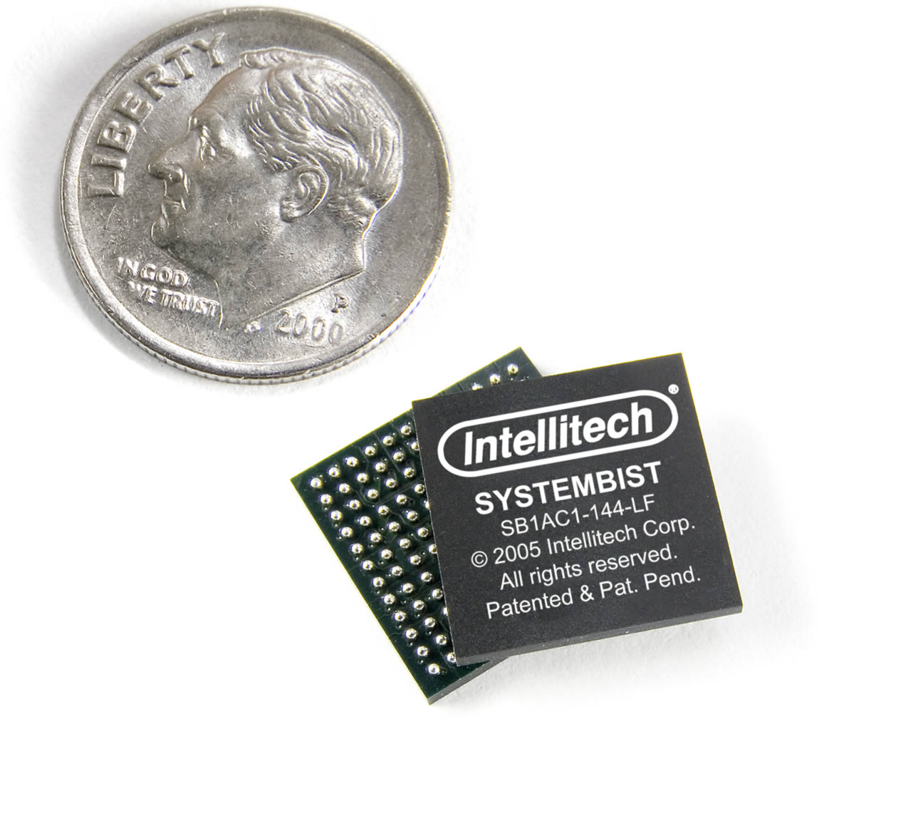
SystemBIST is a complete plug-and-play IC for flexible FPGA configuration
and embedded JTAG test built
upon several unique patented architectures. SystemBIST
is a code-less configuration device which enables design
engineers to build high quality, self-testable and
in-the-field re-configurable products. SystemBIST is vendor
independent and can configure any IEEE 1532 or IEEE 1149.1
compliant FPGA. System CPLDs, EEPROMs and FLASH can also
be re-programmed in the field with SystemBIST through other members of
Intellitech's TEST-IP family. |
|
 |
SystemBIST also provides the worlds first deterministic BIST (Built-In Self Test)
for PCBs and entire systems. SystemBIST BIST removes much of the work required for a system level BIT (Built-In-Test) created with firmware/software. SystemBIST re-uses the manufacturing JTAG/IEEE 1149.1 based test patterns and
scripts and embeds them in the PCB. The tests and FPGA configuration choices are stored compressed in FLASH memory enabling PCBs to be tested anywhere that they
can be powered.
Find out how SystemBIST helped LTX with their on-board FPGA
configuration and test strategy here: SystemBIST simplifies FPGA configuration. See SystemBIST in Xilinx XCELL Journal.
Read the white paper on Business considerations for FPGA based PCBs. The white paper presents information on FPGA security, trojan bitstreams, PCB cloning and other factors designers should be aware of when designing PCBs with FPGAs. AES encryption doesn't prevent trojan bitstreams from being loaded into your commodity FLASH or FPGAs. FPGA Security |
The animation below depicts how SystemBIST and the supporting development
tools will enable you to implement flexible FPGA configuration with CPLD
updating and optional embedded boundary-scan test. Right click over the image
below to play, rewind or forward the Macromedia flash
presentation.
PROM-Based FPGA configuration is no longer economically feasible for designs that have several large FPGA devices
Ever-changing customer requirements are driving the need for product OEMs to deliver designs that are highly
flexible and extendable. This has led to a growing focus on
designing systems that use re-configurable FPGA and CLPD devices. In
the past, when a small number of FPGA devices were employed on a PCB
a simple configuration PROM was more than adequate to configure the
devices at power-up. Given the rapid rise in FPGA size and
complexity a PROM-based configuration solution is not economically
feasible due to the large number of PROM devices required to
configure large FPGA devices. A fairly complex PCB with three
high-density FPGAs can call for $50 or more in re-configurable PROM
parts which occupy more than 2.25 square inches of PCB area.
SystemBIST provides FPGA configuration, CPLD re-configuration and JTAG based PCB self-test for a fraction of the cost.
|
|
"I started to design my new PCB with XC1800 series configuration PROMS, I changed my design to use
SystemBISTTM for on-board FPGA configuration and embedded test when I saw the cost and test benefits for
LTX."
|
|
|
Zack Matisis
Chief Engineer
LTX Corporation
|
 |
Customized in-system configuration solutions use valuable engineering time
The issues surrounding PROM-based configuration are driving design engineers to explore other methods to configure both FPGA and CPLD devices in-system from a centralized source. Many teams have turned to 'home-brewed' customized solutions that leverage on-board commodity FLASH memory to store configuration data and a microprocessor or CPLD to sequence the
configuration bitstreams into the FPGA directly. While these methods can work, they have many drawbacks including:
- Larger PCB area overhead than SystemBIST
- Conventional FLASH memory storage for bitstreams is significantly larger
than SystemBIST storage requirements
- Lack of Flexibility, CPLD/FLASH, Serial PROMS, and Enhanced Configuration
Devices all are simple sequencers, lacking decision making and error handling
- Lack of FPGA programming coordination with boundary-scan techniques affects test coverage
and increases test development difficulty
- Requires expensive software development and support requirements as code must be written and integrated each time the solution is used
- Degrades performance during simultaneous system boot and configuration due to the high CPU activity
- Offers poor ROI as the 'in-house' solution based on system functionality is typically not re-usable or
robust.
- In-the-field updates are at risk as typically configuration PROMS and platform FLASH have to be entirely erased to perform an update. Mission mode operation is interrupted to perform the update.
- Reading Application notes to solve problems still puts critical elements of a project, such as security, at risk for possible vulnarabilities.
|
|
Intellitechs embedded test solutions provide us with a code-less
method to implement embedded test and re-configuration that lowers our overall
system cost.
|
|
|
Pete Marconi
VP of Systems Engineering
Axiowave Networks
|

|
The SystemBIST Processor provides a standard unified methodology for in-system configuration and test
The SystemBIST processor is a codeless
standardized plug-and-play device that does not require resource intensive software
development or impact the CPU during system boot-up. SystemBIST removes configuration
Proms and other glue logic needed for in-house FPGA configuration methods.
SystemBIST employs a unified approach to in-system configuration and
manufacturing test so that a single SystemBIST processor at power up
or under CPU control can configure all programmable logic in the
system and automatically run the entire manufacturing test stream
including Scan, Logic BIST memory BIST and Board Interconnect.
SystemBIST and the associated software makes in-the-field updates 'failsafe', you never need to erase the entire FLASH to perform an upgrade. SystemBIST's built in JTAG tests, allow you to interrogate the status of I/O pins to make sure your FPGA was reconfigured succesfully before finalization.
|
|
Boundary scan is the platform on which board-level BIST will be built. BIST can potentially do for functional test what in-circuit test did for the old instrument-level production electrical test. Given the exponentially increasing complexity of boards, there will come a time when, if you don't have BIST, you won't be able to debug future boards at all.
|
|
|
|
Dr. Kenneth P. Parker and Dan Zimmerle, Agilent Technologies
Article in EP&P, 7/1/2002
|
SystemBIST Benefits
Cost effective
SystemBIST is a single IC that efficiently leverages existing system FLASH memory to hold up to fifteen unique FPGA configuration and manufacturing test suites that can be applied at power-up by SystemBIST. No configuration PROMs are required.
Vendor independent
SystemBIST is a complete vendor independent solution that can be used for in-system configuration of
any 1149.1/1532 compliant FPGA and/or CPLD devices. Unlike PROMS, SystemBIST can also perform field updates of your CPLDs.
Failsafe field updates
Proms and Platform FLASH require the entire device to be erased to perform an update. Proms also require embedded software that you have to create to perform this erasure. Proms are updated through 1149.1, requiring your own embedded JTAG controller or roll your own embedded JTAG software. SystemBIST has an easy to use Failsafe method for in-the-field updates never requiring the full erasure of FLASH, your original FPGA designs are protected. And only SystemBIST can perform the tests needed to make sure your FPGAs did update correctly - PlatformFLASH, SystemACE or Proms can't do that.
Valuable Debug tool
SystemBIST's PC/Solaris based toolset provides design engineers a valuable prototyping aid that can be quickly deployed in the lab to validate functional, test, and debug configurations.
Centralized 'anytime'/'anywhere' in-system configuration and test
SystemBIST is used with the EclipseTM Test Development Environment to create, validate and load system configuration and test suites from a single source. Centralization of configuration and test data greatly simplifies system upgrades. FPGA bitstreams and test suites can be quickly loaded into on-board FLASH memory using
Eclipse and the patented Fast Access Controller (FACTM)
greatly simplifying the updating process.
Built-in self-test and diagnostics
Design teams can lower their overall
development costs by embedding manufacturing test and diagnostics
into their systems. SystemBIST removes the requirements for external
ATE; enables anytime-anywhere testing, descriptive diagnostics are
embedded into the system and automatically run at power-up, test
re-use is enabled -- the same tests can be used throughout the life
cycle of the product including at system integration, HALT/HASS
testing, at customer power-up, field service and depot repair.
Anti-tamper and electronic counterfeit protection
SystemBIST now has on-chip security IDs, a unique 128bit number, customer specific number, EMS/CM number and SHA256 secure hash of these values which may be accessible via SPI or JTAG. SystemBIST provides system-wide anti-cloning, anti-tamper FPGA security with bitstream Trojan protection, secure updates-in-the-field without using FPGA PUFs or extensive logistics in manufacturing. 128-bit security ID
|