Cluster Test Development with JTAG Timing debugger
EclipseTM Test Development Environment enables test engineers to view and debug their test programs in real-time using a logic analyzer and data spreadsheet viewer.
Developing working 1149.1 compliant test programs for PCB's is often a complex task because of the amount of data that is involved. The Eclipse Timing Diagram Analyzer and accompanying Device Spreadsheet Viewer simplify test development because they provide a powerful and highly efficient test program debug platform that displays actual test data and instructions as they are being shifted through each 1149.1 device within the system or board under test.
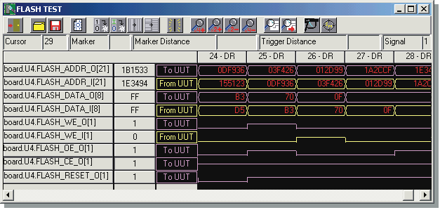
The Device Spreadsheet Viewer provides the user a spreadsheet like form that can display the states of individual device pins or that of a user-defined group of signals within the 1149.1 scan chains. To simplify test program debug even further, the active test instructions within a device as well as the actual and expected data are also displayed. All data displayed in the Device Spreadsheet Viewer is under user control.
 Eclipse Timing Diagram Window
The Timing Diagram Analyzer augments the Device Spreadsheet Viewer and displays bus and register data directly to a graphical timing diagram. The timing waveforms are dynamically updated as data register and instruction register scans occur in the actual design. The Timing Diagram Analyzer also has the ability to set specific triggers based on complex Boolean qualifiers.
Device Spreadsheet Viewer and Timing Diagram Analyzer provide a Test Engineer with a Visual Debug Solution for Today's Complex PCB's
- Signal grouping
- Automatic isolation allow users to view only failing signals
- Simple point and click signal selection
- Save and recall debug scenarios
- Logic analyzer capabilities like complex triggering based on logical operators and movable display markers
- Fast signal search mechanism
|