Boundary-Scan Test for memory interconnects
Memory Test Overview
To produce high-quality products that employ memory devices it requires that each individual memory's interface - address, data, and control pins - be thoroughly tested during
production PCB test. Manually developing high-coverage tests that verify the proper connection of address, data and control signals is a tedious and error prone process. This fact has driven many OEMs to test memories on PCBs from adjacent boundary-scan devices.
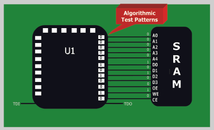 Memory Interconnect Test
Automated Boundary-Scan Test for Memory Interconnect with Eclipse
Intellitech's Eclipse Test Development Environment provides automatic test generation
for shorts and opens tests to memory devices through boundary-scan. The Eclipse Test Development Environment automatically creates tests that detect pin faults for a wide range of memory types.
Key to proper diagnostics, Intellitech's proprietary memory test algorithms pin
point opens and shorts faults other "galloping ones" or "marching ones" tests
miss. .
Proprietary Boundary-Scan to Memory Test Algorithms
The Eclipse Test Development environment is unique in the industry. Eclipse employs proprietary test generation algorithms that can test for shorts, stuck-at and opens pin connections. Other 1149.1 based tool vendors use simple walking '1' and '0' data patterns to test memory interconnect. Testing and accurately diagnosing open pins on a memory's address lines can be challenging due to the unpredictability of the behavior a memory that has a faulty connection. In many instances, the open pin is impacted by activity on adjacent pins that can cause it to float high or low. The proprietary memory interconnect test algorithms in Eclipse are able to accurately detect and diagnose open connections on memory address and data lines.
Accurate Diagnostics
The Eclipse Test Development Environment uses an EDIF 2 0 0 netlist from the CAD development system. This enables Eclipse to provide more robust diagnostics when a memory test fails. For each failure, Eclipse will display the failing component and pins, their corresponding net names and the boundary-scan pins where the failure can be observed.
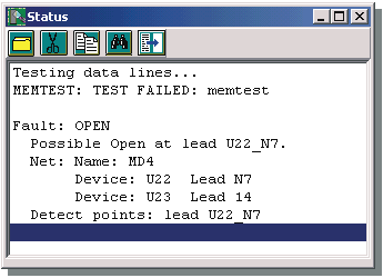 Eclipse Status Window Displaying an Open Fault on a Memory Data Line
Using an EDIF netlist also permits Eclipse to perform constraint checking on pins so that when an engineer is debugging a memory failure with the Schematic Logic ProbeTM (SLPTM) they will not inadvertently set conflicting states on bi-directional or tri-state structures and damage their memory devices.
Extensive Model Library
The Eclipse Test Development Environment has a large library of memory components that describe how each device is written to and read from - read and write protocols. The standard Eclipse library includes device models from AMD, Atmel, Catalyst, Cypress, Fujitsu, Intel, Macronix, Microchip, Micron, SST, ST, Toshiba, Xicor.
Eclipse Memory Test Features
- No special software package is required, the standard Eclipse Test Development Environment supports automatic memory interconnect testing
- Memory tests can run directly from the Eclipse Test Development Environment GUI or can be scripted for easy repeatability in a production
PCB test environment
- Highly automated system, the user does not need to specify low level details such as memory write/read protocol or 1149.1 scan sequencing to create and apply memory interconnect tests
- Eclipse Test Development Environment provides interactive features such as single step -- to help verify and debug basic memory operations
- Unique algorithm assures that DRAM refresh times are met
- Superior fault diagnosis tools - enhanced pin fault report, SLP and Visual AnalyzerTM (VFATM)
- Upload and download memory data to and from a file
- High coverage tests for data and address
pin stuck-at faults, control pin faults, open faults on address
pins and bridging faults on address and data pins
|