JTAG
TEST Intellitech's Eclipse(TM)
Family of Products is a complete Solution for Design Debug,
In-system Device Configuration and Automated Test Program
Development for complex PCBs and Systems. The Eclipse
Family provides design and test engineers with a comprehensive
set of tools that they can use to create, validate and apply
1149.1 (JTAG) based system configuration and test
suites. All tests can be passed to SystemBIST for
embedded test, to Teradyne ICT or to Intellitech manufacturing systems. The Eclipse family has an extensive line of
ultra fast hardware and integrated software options for 1149.1 (JTAG) test and configuration.
|
|
The Eclipse Family is a comprehensive test
solution that reduces product development costs, speeds
time-to-market and improves product quality. Eclipse products enable
companies to develop and execute manufacturing tests and perform
in-system device programming and configuration using the IEEE 1149.1
test infrastructure.
 If you can read a schematic, you can use Eclipse JTAG Test Software
IEEE 1149.1 is an industry standard test
protocol that sometimes is incorrectly referred to as JTAG after the
original European Joint Test Action Group (JTAG). Today's
1149.1 technology uses boundary-scan cells on device IO pins to
provide virtual access to key nets and pins within a printed circuit
board. This enables what is called "ATPG" or automatic test pattern
generation. The ATPG is used to quickly generate tests for a
PCB to check the IC-to-IC interconnects. With Eclipse, the
pattern sets are known to be 'deterministic' which is a fancy word
meaning that the test patterns generated have a pre-determined fault
coverage on the PCB and have a pre-determined diagnostic to the IC
pin. This should be contrasted to 'functional test' which is
non-deterministic, the fault coverage cannot be mathematically
determined with functional test and the diagnostics are not isolated
to the pin.
|
|
"Placing pads for test based on physical access is no
longer an option for us; it increases PCB layout time and decreases
routing efficiency. Intellitech's boundary-scan technology allows us to continue to get high digital test fault coverage without test
pads."
|
|
|
Zack Matisis
Chief Engineer
LTX Corporation
|

|
The automated PCB interconnect testing in
Eclipse is the fastest and most cost effective way to develop tests
for PCBs with high digital device content. It eliminates
the need for manual test development of IC-to-IC connections
and eliminates adding test points late in the PCB design
cycle. These IEEE 1149.1 tests are applied using cost-effective
hardware and software. PCBs that have a high digital content that can be tested and configured through 1149.1 may benefit from using the Eclipse Scan Executive manufacturing environment. If a PCB has long digital test times (including programming FPGAs, CPLDs and FLASH) relative to the analog test times, cost savings can be realized by performing the tests seperate from ICT.
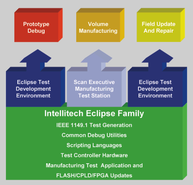
Eclipse Flow Supports Test Reuse throughout the Entire Product Life Cycle
IEEE 1149.1 test and device configuration
data is created, debugged and validated in the lab during product '
bring-up'. Tests created with the Eclipse Test Development
Environment are portable directly to the Scan Executive
Manufacturing Test Station for execution in a production
environment.
The Eclipse Test Development environment is also the platform for creating embed-able 'images' for on-board self-test. This enables the same high coverage tests used in manufacturing to stay with the product when the product is shipped to customers or next level system integrators. The Eclipse Test Development Environment can be used in the field to apply FLASH program updates or re-configure FPGA and CPLD devices.
JTAG for Debug
Design Debug and Bring-up
The Eclipse Test Development Environment automatically creates tests that are used to bring up new products in the lab. Failures can be quickly debugged using software tools such as the Eclipse Timing Diagram Analyzer and the Schematic Logic Probe.
JTAG for Test
Manufacturing Test
The Scan ExecutiveTM Manufacturing Test Station is used to apply the same IEEE 1149.1 tests that were developed and used in the lab in a high-volume manufacturing environment without requiring additional development.
JTAG for re-configuration
Field Service
The Eclipse Test Development Environment is used at a customer site or in a repair depot to debug failures and update and re-configure existing products.
Eclipse Family of Products
Eclipse Test Development Environment - is a complete solution that provides support for: automatic test pattern generation, interactive graphical debug and fault resolution, in-system device configuration, FLASH programming and boundary-scan based memory interconnect testing.
Test data from the Eclipse Test Development Environment is applied to PCBs or systems though the 1149.1 test bus using Intellitech's Intelligent Test Controllers.
Eclipse Scan Executive Manufacturing Test Station - is an easy to use specialized software platform that enables manufacturing personnel to control the application of 1149.1 manufacturing test programs and in-system device configuration suites, that were created with the Eclipse Test Development Environment using Intellitech's Intelligent Test Controllers.
Intelligent Test Hardware - UltraTAPTM, RCT IITM, PCI ScanLabTM are high-throughput, fixtureless, cost-effective digital test hardware solutions that apply test data using the IEEE 1149.1 test bus.
Eclipse Family Benefits
-
The Eclipse Family provides a cost effective platform for
applying digital test and configuration
-
The Eclipse Family provides a single software
platform for manufacturing test development, debug and application
for complex ICs, PCBs and Systems
-
The Eclipse Family leverages industry standard IEEE
1149.1 methodology to ensure that same test data can be used in
design, on-board, manufacturing and field
-
Eclipse Family provides high fault coverage which
reduces overall product development costs
-
Eclipse Family reduces the amount of time it takes
to bring up a new design and move it to volume production
-
Eclipse Family provides efficient in-system JTAG
FLASH programming and FPGA/CPLD Configuration
-
Eclipse Family is integrated with the TEST-IP
Family of Infrastructure IP for a complete embedded configuration
and test solution
|