Production PCB Test and
Environmental PCB test strategy reduces costs
PT100 Parallel Tester - Industry's
highest throughput digital test and configuration tester
The PT100 Parallel
Tester enables high
throughput PCB digital test, on-board FLASH and CPLD
programming while keeping up with modern production line rates
of one PCB every 20 to 40 seconds. The PT100 is a key
element in any modern CM or EMS manufacturing line. As
test time and in-system configuration times continue to
increase, the PT100 can keep up with the fastest production
line without sacrificing on product test quality or resorting
to pre-programming non-volatile parts. The
PT100 Parallel Tester is designed to off-load in-circuit
testers and in-line programmers and optimize throughput of
digital test and configuration of PCBs incorporating the IEEE
1149.1 standard. It
is ideal for testing large FPGA based PCBs with moderate to
large amounts of FLASH memory or panelized PCBs with 8, 16, 32
or more circuits per panel.
Click here to download a copy of the white paper "New
Strategies for cost effective production PCB test and configuration"
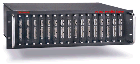
Each PT100 chassis can support up to 16
boundary-scan controllers all managed by a single production
test software running on a PCI or PXI based
PC. Each PT100 chassis can be connected to as many
other PT100 chassis that are necessary to optimize throughput
and reduce overall programming and test
times.
The Intellitech PT100
Parallel Tester is based on Intellitech's patented Concurrent JTAG or CJTAG (See CJTAG White paper), which enables low cost simultaneous test
and configuration of an unlimited number of UUTs (Unit Under
Test) over common industry busses such as IEEE 1149.1. While the UUTs are
configured and tested simultaneously, individual access to
each UUT is preserved, for instance a unique serial number or
MAC address could be programmed into each UUT during the
parallel test and configuration process. The tester uses a
second patent-pending technique to balance test times with UUT
handling times to optimize the throughput and match the beat
rate of a production line without complex line balancing and
duplication of capital equipment. The tester is targeted for
CMs and OEMs that make medium to high-volume digital consumer
products such as PDAs, Cell phones, Cable set top boxes, or
other applications where digital test and configuration times
using IEEE 1149.1 affect PCB test
throughput.
|

|
|
|
Figure
1. Traditional ICT
focused flow
|
|
The traditional test flow for PCBs with
FLASH and BGA devices is shown in
figure 1. Variations of this flow include pre-programming FLASH memory
and CPLD devices then creating an storing in inventory rather than
programming in-line. In this flow, in-circuit
testers such as Agilent and Teradyne perform
boundary-scan (IEEE 1149.1) test with built-in software or
a third party boundary-scan controller is incorporated into the
in-circuit tester. In the past when PCB
digital test times were short, that is, roughly equivalent
to the analog test time of a PCB, using boundary-scan on
ICT was an efficient strategy. However,
non-volatile devices (FLASH, EEPROM, CPLDs, etc) continue to increase
in size and use in the modern PCB.
These devices increase the digital test and configuration
time of the PCB such that this creates a bottleneck on
the in-circuit tester. Even with direct physical access
to FLASH memory, some devices can take as much as 45 seconds
or longer to program.
-
Typical boundary-scan test and configuration
(programming CPLDs, FLASH etc) on a "C" size PCB can take
60-90 seconds.
-
A Cisco PCB w/ boundary-scan test takes
approximately 3 minutes to
test
-
A 4 CPU network server takes roughly
3 minutes to execute 1149.1 tests and at-speed memory
tests
-
A single Intel 28F128J3 StrataFLASH with full
pin access takes ~144 seconds to
program. The latest Intel 28F128K3 StrataFLASH takes ~78
seconds to program.
As
digital test times have increased, the utilization of the ICT
during the testing has dropped, in many cases the ICT is just
supplying power while a independent boundary-scan controller
applies test and configuration data.
|
 |
|
|
Figure 2. Optimized Flow for new
generation PCBs |
|
As
digital test times have increased, assembly test flow can be
optimized by testing more UUTs in parallel.
On-board programming of FLASH through 1149.1 has received much
attention, however, on many PCBs the FLASH configuration times
over a single 1149.1 controller is unacceptable, forcing
pre-programming or in-line FLASH programming equipment.
ISP (In-system programming) of CPLDs is also desired, but adds
to the digital test time.
New high-speed technologies and at-speed
structural test (testing IC to IC connections with 1149.1 at
there rated speed) require testing connections without
pogo-pins.
+FPGAs with gigabit serial
interfaces from Altera and Xilinx
+SDRAM, FCRAM, DDRAM
memories require at-speed testing
+ AC coupled
connections (when a capacitor exists betwen boundary-scan
connections) require precise timing to test over 1149.1 or the
1149.6 standard
+ IBIST -
Interconnect Built-in Self-Test or 'at-speed'
interconnect
testing
Figure 2 shows the optimized flow of testing the
modern PCB. Parallel 1149.1 test enables testing and
configuration of the largest PCBs within the beat rate
of the production line with a minimal of capital
equipment.
Environmental
test
Environmental testing
(exercising the system or PCB over temperature and humidity)
typically is the longest test process of any product.
Since the tester can test many PCBs in parallel, it is an
attractive alternative for testing large number of PCBs
in an environmental chamber when the Intellitech embedded test
products (SystemBIST) cannot be used. The PT100 sets a
new price point enabling lower cost, high-volume products to
be tested over temperature that typically could not be
justified.
PT100 expandable
architecture
The tester itself is
not a traditional tester with a back plane and fixed number of
test channels, but a collection of self-contained 'parallel
tester card' building blocks that connect together over
flexible ribbon cable. The PT100
Parallel Tester cards are housed in a 19" 3U height rack
mountable box with room for 16 plug-able cards, each one
supporting 24 re-configurable tester channels and one IEEE
1149.1 controller.
Each 19" rack of 16 parallel tester cards can then be
connected to another 19" rack of PT100 tester cards, expanding
the tester channels as physical space and AC power
permits.
The physical flexibility of
the tester enables it to interface with a variety of UUTs from
small cell phones to large telecom blades. The 24 tester channels
and 1149.1 interface have a programmable logic high output
level from .8v to 5V with a current drive of up to 84ma. The IEEE 1149.1
interface can deliver and test boundary-scan data to and from
the UUT at 64 Megabits per second on each tester card
simultaneously.
Each tester card also has a high-speed clock channel
that supports a clock rate up to 500Mhz for use with at-speed
Built-In Self Test on the UUT.
The tester cards are
controlled from a single PC console using either Intellitech's
PXI or PCI card interface and Intellitech's Scan Executive
manufacturing software. The software comes standard with
integrated support for adding PXI, GPIB or VISA instruments
and power-supplies needed for testing the UUTs. A secondary
connector exists with auxiliary I/O that support integrating
the parallel test process with automated board handlers and
external fixturing.
Test development and debug is done with the Eclipse
Test Development Environment. All the tests
developed for testing a single PCB can be exported without
modification to the Intellitech Parallel Test
environment.
Benefits
-
Maximizes PCB configuration and test throughput for
production or environmental test
-
Users
can parallelize PCB
test and FLASH programming and not parallelize production
lines
-
Provides a solution for matching PCB test and
configuration throughputs to the beat rate of the production
line.
-
Designed to off-load in-circuit testers and in-line
programmers using patent-pending parallel test
methods.
-
Reduces costs by eliminating complex line balancing and
duplication of capital equipment.
-
Enables the balancing of test and configuration time
with UUT handling time.
-
Enables structural test during burn-in testing for high
volume products
-
Enables
higher fault coverage tests without sacrificing test
throughput
- Can apply and diagnose JTAG/1149.1 tests from 3rd party vendors. No need to 'switch' vendors. (read more )
|