|
PinFault Diagnostics
The Eclipse Test Development Environment displays in real-time PinFault Diagnostics information in a Status Window when a failure occurs during PCB test. In many cases, standard PinFault Diagnostics provides the user with enough information to resolve failing tests. Boundary-scan Intelligent Diagnosis (BSID) is run when more information is required to diagnose a failure.
For each failure, PinFault Diagnostics lists the device name and pin where the failure was observed. The Schematic Logic ProbeTM (SLPTM) can be used to examine the states of adjacent nets to aid in fault isolation. The scan bit position where the failure occurred is also displayed in the PinFault Diagnostic Report. This information is helpful when using other Eclipse debug tools such as Timing Diagram Analyzer or the Spreadsheet Viewer.
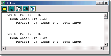 Eclipse Status Window Displaying Faults on U3 pin P41 and P40
|