Boundary-scan enables interactive schematic viewer and pin toggler
Schematic Logic ProbeTM (SLP) is the aggregation of two traditional design debug tools into a single software package that enables design and test engineers to quickly resolve problems on PCBs that employ an IEEE 1149.1
Boundary-Scan test methodology. SLP enables engineers to interactivity probe and set logic states on the pins of the Unit Under Test (UUT) from within a virtual debug environment.
Unlike paper schematics or "design browsers," Schematic Logic Probe is dynamic: components and nets are not fixed to a particular page or location. During a debug session, SLP quickly displays the "interesting" components in a virtual schematic view so that engineers do not have to page through large schematics in order to find their debug objectives. SLP is more than a viewer; it enables engineers to probe and control the state of pins and nets directly from a virtual schematic view to isolate problems on the UUT.
Using Boundary-Scan (JTAG) 1149.1, SLP 'scans' the components and pins updating
logic values on pins and nets throughout the entire design.
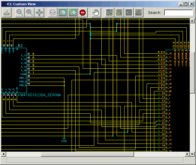 Schematic Logic Probe Window
Debugging with SLP
Initially, SLP reads an EDIF netlist and creates a database. During the design debug proces, SLP extracts specific connectivity information from its database based on the pins and nets that the engineer is interested in probing. Next, SLP takes that information and uses its advanced placement and routing algorithms to create a virtual schematic view that displays only the drivers and receivers the engineer wants to control and observe.
*By clicking on the underlined links in the text below you will be able to see a demonstration of each feature. The demonstrations are best viewed in a full screen browser window.
SLP creates customized debug views of selected objects in numerous ways:
Show Selected Components - SLP displays only the components that you select
Show Devices with Selected Pins - SLP displays a debug view showing only the user selected components
Partial Device View - Many devices have too many pins to enable easy debug and viewing. SLP partial views allow you to highlight and select just the buses and pins you needed to debug. Other "design viewers" lack the ability to break down a large device into smaller views, making it too cumbersome for debug today's high pin count devices.
Show Selected and Connected Devices - SLP displays the components you select (either complete or partial) along with all connectivity to other devices.
Search by Type, Device, or Net - SLP displays a virtual schematic containing the items that were found in a database search.
SLP includes other powerful features for interactive debug:
Reset - SLP can reset the UUT
Drive Data - SLP allows interactive control of device logic pins. Simply clicking on the schematic view of the pin allows the engineer to modify the logic state of two state, three state and bi-directional drivers in the design.
Observe Only - SLP enables a non-intrusive 'snapshot' of a PCB or System's logic values from its functional state
Observe Loop - SLP can continuously monitor all logic pins in a design without impeding the system operation.
SLP uses an easy to read color-coded scheme for displaying data from the UUT. SLP color-codes each device pin based on its ability to control them:
Turquoise - SLP cannot control these pins
Green - Input pins that SLP cannot control
Orange - Output pins that SLP can control
Grey - Disabled pins that SLP can control
SLP color-codes each pin's state:
Green - Represents the actual logic value on the pin
Yellow - Represents the logic value that was pin values captured from the core logic
Grey - Represents a disabled pin
Red - Represents different driving and capturing logic values a indicating a fault in the net
SLP also has zooming and printing capabilities.
Boundary-Scan based Schematic Logic Probe Benefits
- Simplest Boundary-Scan interface for PCBs with IEEE 1149.1
- Simplifies large designs with non-searchable PDF schematics
- No more paging through cumbersome paper schematics
- Boundary-Scan 'SAMPLE' mode enables Non-intrusive probing (observe-only) to quickly find bugs
- Boundary-Scan "EXTEST' mode enables 1149.1 device pin toggling with
instant feedback of net logic levels
- Isolate complex problems with the simultaneously display of N nets
- See exactly what is happening in your design, values are color coded for easy interpretation
- Debug faults by setting logic values on all two-state, three-state and bi-directional output pins
- Break-up large pin count devices to manageable smaller views
- Fast productivity, SLP reads output of all major PCB Schematic Capture Software
- Cross probe to PCB layout (Physical View) with Visual Fault Analyzer
|