Problem
CPU and micro controller based designs often employ FLASH memory to store a system's firmware because of its flexibility. Many product teams have adopted a strategy that programs their FLASH devices in-system.
Standard IEEE 1149.1 test infrastructure and the EXTEST instruction can be used to program FLASH devices in-system. This technique has limited impact on the design and only requires that the FLASH memory's address, data and control signals be directly connected to an 1149.1 compliant device so that device's boundary register can be scanned during each FLASH write sequence.
Programming FLASH devices in-system using 1149.1 has serious performance issues
- Today's designs employ numerous large pin count boundary-scan devices which impact the length of the scan path
- Signal integrity issues limit TCK frequencies which impacts in-system programming times
- Access to the WE, Ready/Busy status pins of a FLASH device is not always possible
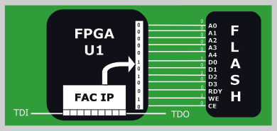
In-System FLASH Programming Solution Using the FACTM
The Fast Access Controller (FAC) is a member of the Intellitech TEST-IPTM family of pre-designed infrastructure intellectual property modules for high-speed, high-throughput, in-system configuration and test. The FAC leverages the 1149.1 test infrastructure to enable in-system programming of FLASH memory devices as fast as off-board or direct access programming techniques. The patent-pending FAC FLASH programming method is scalable, it can still achieve this optimal FLASH programming throughput with low test clock rates (<3Mhz) and is unaffected by the size or number of 1149.1 devices in the boundary-scan chain design of the PCB.
FAC eliminates performance issues associated with 1149.1-based in-system FLASH programming
- FAC programming performance is independent of length of the scan path
- FAC is not impacted by the TCK frequencies
- 1149.1 access to the WE, Ready/Busy status pins is not required with FAC
The FAC is an ideal plug-and-play IP solution for processor (Micro-controller, DSP or CPU) designers who need to respond to customer demands for better Design-for-Test and better support for programming external FLASH in a production environment. ASIC/SOC designers using embedded CPU cores from ARM, MIPS, IBM and Motorola can also lower overall product costs by using the Fast Access Controller to lower downstream PCB manufacturing costs. ICs within high volume, low cost consumer products that leverage large quantities of non-volatile memory such as cell phones, PDAs, and cable set top boxes can particularly benefit from the FAC.
The FAC IP can also be embedded into an FPGA so it is an attractive alternative for PCB designers who are under pressure from their test engineering groups to provide direct physical access points for FLASH memory devices so manufacturing can realize shorter programming times. It is also particularly useful for FPGA based PCBs that use on-board FLASH as a method of storing FPGA configuration data. The FAC enables the IEEE 1149.1 bus to be used as a central high-speed serial bus for in-system configuration of all on-board FLASH devices.
The FAC IP achieves its fast on-board programming times by using advanced data de-serialization and protocol optimization algorithms to minimize the number of scan operations and data required during FLASH programming. This enables the FAC to program FLASH devices in-system over the standard 1149.1 bus at speeds equivalent to off-board programming. The FLASH memory protocols of the FAC are fully configurable in-system, using Intellitech's EclipseTM family of 1149.1 based tools allowing it to support a wide variety of FLASH memory devices and protocols from vendors such as Intel and AMD.
 Fast Access Controller (FAC) embedded into a processor
Intellitech's SystemBISTTM Embedded Configuration and Test Processor can be used with FAC to provide users with a complete embedded solution for in-system FLASH programming and configuration of CPLD/FPGA devices. SystemBIST enables manufacturing tests (PCB and PCB to PCB) to be developed, validated and embedded directly into the system. Embedded Test eliminates the need to run digital tests and device configuration using ICT. Embedded test also permits the same set of tests to be used in lab prototyping, volume PCB manufacturing, System Integration, HALT/HASS tests, at customer power-up, field service and depot repair. System re-configuration could take place anywhere so that engineering changes could be easily made at any point in time during a product's life cycle.
|