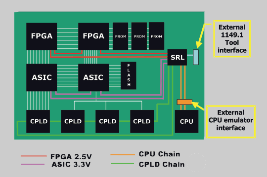
1149.1 JTAG Mux Switch
The SRL is a complete plug-and-play IC that can be easily incorporated on a PCB to reduce the complexities and costs of designing IEEE 1149.1 test infrastructure for designs that use multiple scan rings. The SRL
links any number of scan rings (secondary scan paths) into a single high-speed test bus, which permits devices on secondary scan chains to be independently tested and configured through a single IEEE 1149.1 external interface. This dramatically shortens scan operations and thus enables
the fastest on-board FLASH programming times, IC silicon debug time and in-system configuration times.
The SRL is critical the success of deploying multi-card systems where JTAG access is needed on each card. The increase in on-chip instruments accessible through JTAG requiest that JTAG access be possible with the PCB in-situ, without using pogo-pin fixtures. Read more about how Intellitech helped Polycom create an easy to use multi-PCB system using the SRL. Polycom Success Using Scan Ring Linker
The SRL provides proper buffering of test signals to reduce the need for external logic and complex interfaces between boundary-scan devices that require different input voltages. SRL is IEEE 1149.1 compliant, fully testable and fulfills all of the requirements for multi-chain PCB design. SRL is more cost-effective than using buffers and voltage level translators which also introduce delays that affect the performance of the system test clock (TCK).
If you need linking with multi-drop JTAG for Systems with backplanes then please see CJTAG
 The SRL creates a single, easy to use, high-speed test interface for multi-voltage scan-chains
Challenges of using complex scan chains
To reduce test and in-system device programming times designers often use multiple scan chains. This enables a single long scan chain to be broken up into smaller chains that are more efficient. Programming and configuration times for FLASH and FPGA devices can be shortened if the devices are placed on smaller scan chains. In many cases, in-system configuration of FPGAs cannot take place unless they are completely isolated in a separate scan chain from other functional logic.
Accommodating multiple voltage level
ICs requires the designer to add voltage translators. Commercial Scan Path Linkers from TI and ScanBridge from NSC have been used as a method of accommodating multiple scan paths. The devices pose significant problems to test engineers who use third party IEEE 1149.1 test development tools. Users are forced into significant manual intervention in order to debug and get working manufacturing tests. These devices also do not support today's lower voltage designs. Signal Integrity must be addressed in the distribution of TCK, TMS and TRST signals. Design and test complexity increases significantly and IEEE 1149.1 expertise is required to integrate and test the system.
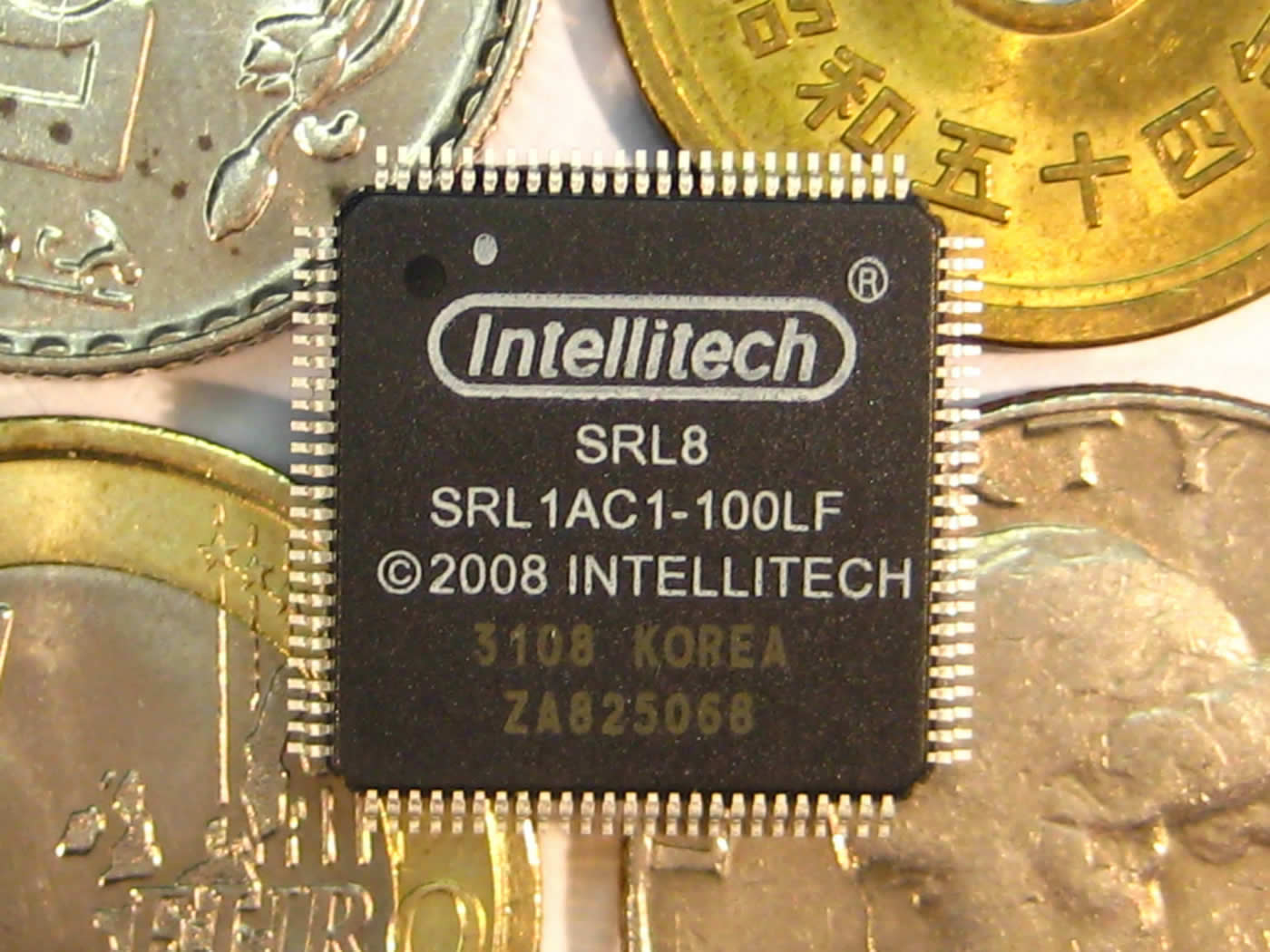
The Scan Ring
Linker is a plug and play solution for designers who use multiple scan chains
The high fanout and
voltage translation fulfills all of the requirements for multi-chain PCB design. The SRL is cost-effective because it eliminates the need to incorporate special buffers and voltage level translator components on the board. The SRL is fully configurable, completely IEEE 1149.1 compliant so it removes the requirement to design and implement a complicated customized test implementation that may not be testable itself.
The SRL pins themselves are fully testable for shorts enhancing fault coverage and diagnostics when scan path problems exist.
The SRL in conjunction with the Eclipse Test Development Environment reduces design bring-up time because it can make system debug using ICE and OCD methodologies much more efficient.
Benefits of the SRL Technology
Reduces part costs
SRL can be deployed as a single IC on a PCB to reduce the need for scan chain buffers and logic level translators. SRL permits devices in secondary scan chains to have their IO pins configured at different voltage levels. A single SRL device controls each scan chain regardless of their voltage.
Better signal integrity
TCK TMS TRST TDI TDO
SRL provides superior distribution of TCK, TMS and TRST signals permitting high-speed test operation. PCB engineering is also reduced as SRL eliminates complex test signal routing.
Faster TCK rates
SRL uses Intellitech's Wide-Capture to enable faster TCK rates than in-house designed CPLD JTAG muxes or commerical parts like ScanBridge or TI 74LVT8997. Wide-capture compensates for slow TDOs that maybe coming back across 12-18" or more of PCB trace back to the SRL. You get 95% more setup time than any other technology available.
Flexible implementation
SRL simplifies design with a simple to use IC or as a plug-and-play IP that is easily embedded into a dedicated CPLD.
High fault coverage
SRL enables high fault coverage for
1149.1 test signals -- TCK, TMS, TDI, TDO. Each TCK, TMS, TDI
and TDO pin plus all buffered copies of TCK/TMS have a boundary-scan cell that can be used to test
for shorts prior to the traditional scan-chain tests
Test-Logic-Reset transparency
The SRL doesn't lose its scan ring configuration when a JTAG Test-Logic-Reset is received. NS STA112 and TI 74ACT8997 do turn off their rings without the user knowing it. The SRL saves time, provides predictable secondary rings and reduces the trouble of needing to continually turn on secondary rings (paths) after issuing a board level test logic reset.
Emulation Tool and FPGA tool compatibility
Intellitech has a patent-pending technique unavailable with any other device that allows the SRL to be transparent to other tools. The SRL secondary rings can easily be selected so your Emulation Tool or FPGA tool (Chipscope, SignalTAP etc) can directly access devices for debug.
|