Intellitech's PT100 Parallel Tester maximizes
PCB
test and configuration throughput
Patent-pending
technology reduces cost of test for PCBs with high
production
line 'beat rates' and long test times
Charlotte,
NC - ITC- (BUSINESS WIRE) - September 30, 2003. - Intellitech Corporation,
the technology leader in scan-based configuration, debug and test
solutions today announced the availability of the Intellitech PT100
Parallel Tester. The
PT100 Parallel Tester is designed to off-load in-circuit testers and
in-line programmers and optimize throughput of digital test and
configuration of PCBs incorporating the IEEE 1149.1 standard. The Intellitech PT100
Parallel Tester is based on Intellitech's patent-pending parallel
test bus, which enables low cost simultaneous test and configuration
of an unlimited number of UUTs (Unit Under Test) over common
industry busses such as IEEE 1149.1. While the UUTs are
configured and tested simultaneously, individual access to each UUT
is preserved, for instance a unique serial number or MAC address
could be programmed into each UUT during the parallel test and
configuration process.
The tester uses a second patent-pending technique to balance
test times with UUT handling times to optimize the throughput and
match the beat rate of a production line without complex line
balancing and duplication of capital equipment. The tester is targeted for
CMs and OEMs that make medium to high-volume digital consumer
products such as PDAs, Cell phones, Cable set top boxes, or other
applications where digital test and configuration times using IEEE
1149.1 affect PCB test throughput.
The tester itself is not a
traditional tester with a back plane and fixed number of test
channels, but a collection of self-contained 'parallel tester card'
building blocks that connect together over flexible ribbon
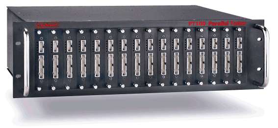
cable. The PT100
Parallel Tester cards are housed in a 19" 3U height rack mountable
box with room for 16 plug-able cards, each one supporting 24
re-configurable tester channels and one IEEE 1149.1 controller. Each 19" rack of 16 parallel
tester cards can then be connected to another 19" rack of PT100
tester cards, expanding the tester channels as physical space and AC
power permits. The
physical flexibility of the tester enables it to interface with a
variety of UUTs from small cell phones to large telecom blades. The 24 tester channels and
1149.1 interface have a programmable logic high output level from
.8v to 5V with a current drive of up to 84ma. The IEEE 1149.1 interface
can deliver and test boundary-scan data to and from the UUT at 64
Megabits per second on each tester card simultaneously. Each tester card also has a
high-speed clock channel that supports a clock rate up to 500Mhz for
use with at-speed Built-In Self Test on the UUT.
The tester cards are
controlled from a single PC console using either Intellitech's PXI
or PCI card interface and Intellitech's Scan Executive manufacturing
software. The software comes standard with integrated support for
adding PXI, GPIB or VISA instruments and power-supplies needed for
testing the UUTs.
A secondary connector exists with auxiliary I/O that support
integrating the parallel test process with automated board handlers
and external fixturing.
Test development and debug is done with the company's Eclipse
Test Development Environment.
All the tests developed for testing a single PCB can be
exported without modification to the Intellitech Parallel Test
environment.
Benefits of the
PT100 Parallel Tester over Boundary-Scan on In-Circuit
Testers
"Boundary-Scan Test on ICT is
a strategy to reduce handling time, where as Intellitech's Parallel
Tester is a strategy to reduce the total test and configuration
time", said CJ Clark, Intellitech's CEO and past IEEE 1149.1
chairperson. "For PCBs with long configuration and test times
relative to the handling time, the highest throughput per dollar can
be achieved more cost effectively by optimizing the test and
on-board programming time, not just the handling time. ICT is a 'one-at-a-time'
approach. PCBs with
long digital test times are better tested in parallel after a simple
analog ICT test or a low cost MDA type test", Clark added.
For certain products,
especially when on-board FLASH or CPLD programming is desired, the
digital test and configuration times can be 10-30 times longer than
the analog test time and the handling time combined. Customers are already
reporting ICT test times greater than two minutes for some
PCBs. Of that
two-minute test time, a small fraction is analog test time for
passives and the remainder is digital boundary-scan test and
configuration time.
This type of PCB may spend 10 seconds or so in analog test on
the In-Circuit Tester and then need 110 seconds of boundary-scan
based test and configuration. If this boundary-scan test is
performed on the ICT, then this approach shifts a lower-cost (IEEE
1149.1) test technique onto the higher dollar ICT capital
equipment. Since only
one or two medium sized PCBs can be tested at a time with this
approach, then multiple boundary-scan on ICT stations are needed to
keep up with the line rate.
This increases the test costs and reduces the
throughput.
Platform for
at-speed and functional test after boundary-scan test
"No one in the industry is
saying, 'Let's integrate AXI or AOI with ICT so we can save a
handling step', as these are different and separate test
techniques", said Clark.
"Integrating boundary-scan controllers on ICT test platforms
should be done with caution, only certain low volume products or
products with short digital test times on ICT that can be performed
fast enough to keep up with the production line rate will benefit
from combining the two test techniques. Without calculating
mathematically which approach to take, you could end up increasing
your test costs by integrating the two."
While boundary-scan test can
be performed on in-circuit test platforms, just because it
can be done, doesn't mean that it should be done. The product type and
product's digital and analog test time should be the determining
factors if boundary-scan on ICT or parallel boundary-scan is the
proper approach. A
product with high digital fault coverage, long on-board programming
times and at-speed test requirements should be considered for test
and configuration separately from ICT. Certain products with
long digital test and configuration times (products with FPGAs,
on-board FLASH or needing at-speed tests) will benefit from being
tested simultaneously with the Intellitech PT100 Parallel
Tester.
"For some PCBs we see IEEE
1149.1 test and on-board programming as separate technique from
MDA/ICT style tests and either a separate step or a step closely
coupled with the functional test," said Clark. "AXI, AOI, parallel
boundary-scan and functional test may be all that is needed for
certain types of PCBs.
Take for instance a CPU based PCB with multiple high
pin-count FPGAs. After AXI and AOI, the PT100 Parallel Tester can
perform boundary-scan structural tests on 25-30 PCBs simultaneously,
then in parallel download CPU based functional test code to the
CPU's FLASH memory, have each CPU execute on-board functional tests
simultaneously, capture the results and then in parallel, erase the
FLASH and download, the product's real operation code" added
Clark. "Even though
this test and configuration may take several minutes, all of this
can be done with a single Intellitech PT100 Parallel Tester keeping
up with a rate of one PCB every 10 seconds" Clark
stated.
"Our customers are already
running at-speed memory tests in the 200Mhz range", said Mike
Ricchetti, Intellitech CTO. "A pogo-pin ICT
fixture is not the environment you want to run these types of tests
on. The environment is
noisy, and each pogo-pin will affect the signal integrity on the
PCB. In addition, the
power delivery is unnaturally distributed over the PCB and is not
delivered the way it would be during normal functional operation.
The subtle differences in in-rush current, the instantaneous current
needed during switching, can affect high-speed testing results. As the need for testing
on-PCB gigabit SERDES interfaces increases, the pogo-pin fixture
will become less appropriate for these types of high-speed tests",
Ricchetti pointed out.
The parallel test patent was
filed in the US and worldwide in July of 2001. "The Intellitech PT100
Parallel Tester's second patent-pending method, called Clark's equation, balances
handling time with test time", added Mike Ricchetti. "Even though the PT100 could
do it, we're not saying you should test one thousand PCBs
simultaneously, that doesn't take into account handling time. In it's simplest form, Clark's equation says that
given a fixed bandwidth for a tester, the number of UUTs that should
be tested in parallel is equal to the test time of the UUT divided
by the handling time. Therefore, for a PCB with 240 seconds of test
and on-board programming and 12 seconds of handling time (to barcode
the PCB and get the PCB onto and off of the tester), the total
number of PCBs to test in parallel is 20. A single Intellitech PT100
Parallel Tester can then keep up with a production 'beat rate' of
one of these PCBs every 12 seconds or more."
More information can be found
at http://www.intellitech.com/products/paralleltest.asp
Pricing and Availability
The Intellitech PT100
Parallel Tester hardware is available now from stock. The base
tester hardware with just four (4) cards is approximately
$9,750.00. Each
additional tester card is approximately $1,800.00. Contact
Intellitech at http://www.intellitech.com
for various options.
Intellitech is a registered
trademark of Intellitech Corp.
PT100 Parallel Tester is a trademark of Intellitech
Corp.
|