Silicon Debug for ICs and SoCs
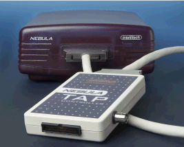
The NEBULA Silicon Debugger is Intellitech's second generation DFT validation and silicon debug platform
Overview
|
NEBULA provides advanced features for performing early validation of
DFT infrastructure and ATPG patterns in first silicon. The NEBULA solution
directly imports test pattern formats and DFT information from leading EDA
vendor tools, such as Synopsys' TetraMAX and Cadence's Encounter Test. The
test information can be imported without translation to NEBULA. NEBULA has
built-in support for gate and net level diagnostics using either TetraMAX or
Encounter Test diagnostic engines.
The NEBULA Silicon Debugger is a silicon debug and validation platform that is
remotely accessible over the network. It enables engineers to accelerate the
debug of prototype IC designs, resulting in faster time-to-volume. With the remote
network access capabilities of the NEBULA platform, design and test engineers
can have debug and test access to first silicon from their office, or from any remote
location.
|
|
|
A Structured Silicon Debug Solution
With increased circuit complexity and advanced packaging, silicon debug is
becoming more difficult. Physical access and visibility into the design for debug
are significantly reduced, especially during prototyping when the silicon is in-system.
As a result, these designs call for structured debug methods that validate
tests that later can also be used by production testers. The NEBULA Silicon
Debugger platform was designed for use with these advanced debug and
diagnosis methods.
Is it fast enough? Structural stuck-at and path-delay tests do not need
high-speed access to the pins of an IC as functional test does. NEBULA takes
advantage of this DFT and performs the same tests with a reduced number of
pins. Even though the production test patterns may need full physical access,
NEBULA provides 'virtual access' and enables debug and modification of these
broadside test patterns without translation.
Validate DFT with Proven Flows
The NEBULA Silicon Debugger can be used to quickly validate DFT infrastructures
such as internal scan, IEEE 1149.1 Boundary Scan, memory BIST and logic BIST.
It enables BIST and ATPG patterns, such as stuck-at and path-delay faults, to
be validated by design and test engineers in a easy-to-use WinTel environment. With NEBULA, engineers
can perform validation as soon as first silicon is available, eliminating the dependency on
the limited availability of high-cost ATE resources.
Benefits
- Provides a debug solution for
complex designs with advanced
packaging, where physical access
is limited and structured debug
and test methods are needed.
- With proven flows, easily import
vectors from Synopsys TetraMAX
and Cadence Encounter Test. No
translations or modifications are
needed.
- Integrated support for TetraMAX and Encounter Test diagnostics to pinpoint silicon
failures to the gate and net level.
- Quickly and easily validate DFT
infrastructure, and production test
patterns. Accelerates debug and
improves time-to-volume.
- Start validation as soon as first
silicon is available. Use to test and
diagnosis first silicon, and to
perform structural characterization.
Eliminates the need for high-cost
ATE during the prototype bring-up
phase.
- Provides ' in-situ' access to debug
features of prototype silicon for
functional debug, where the IC is
on a board or in the system.
- Enables debug of production test
patterns in a 'in-situ' or reduced pin
contact environment without test
pattern translation
- Re-useable test and debug scripts
throughout the design hierarchy, silicon revisions and within
different test environments saves time and reduces development
costs.
|