|
What is touch time? All the infrastructure design, debugging, testing, handling,
revision support and other engineering tasks that occur from product
definition to final product shipment.
Read about these engineering management examples:
- Valuable engineering face
time is taken during the project's critical path to design and debug
home-brew FPGA configuration solution. The schedule slipped and the parts
cost increased
- FPGA vendors have made it
so easy to design the big blocks of the system, the PCB infrastructure
to make the system a viable product, is taking as much time if not
more to design, route and debug.
- The engineering team lost
time and beta customer confidence debugging a failed method for updating
the FPGA designs in the field which didn't properly account for
different silicon revisions.
- Our PCB was designed with
numerous local commodity FLASH for FPGA configuration. The long
download time in the lab adding to engineering time. Programming the
FLASH through JTAG was too slow for the CM so they resorted to
pre-programming FLASH, inventorying sufficient FLASH, and updating
inventoried FLASH each time with the latest revision. The numerous FLASH
and inventorying increased our material costs.
- The PCBs tested OK at the
contract manufacturer but failed in the system chassis at elevated
temperature - engineering time increased, daily teleconference
meetings, and cost of effort increased.
- The CM was in multiple
countries - each location needed to purchase multiple PC based JTAG
stations and each needed on-site help with the JTAG test setup. The effort doubled when we added JTAG
tests during burn-in. The
production schedule slipped, costs increased.
- The CM doesn’t have
time to learn the details of our system functionality so they can't
trouble-shoot functional tests well, especially high-speed SERDES and
DDR. The functional tests do
not provide enough granularity to isolate the
fault and improve the production solder process.
- The functional tests
represented a high man-hour investment however they failed to identify
a hardware problem in the field – lost engineering time and
credibility with customer. Functional test development was a high-risk
investment as there was no payoff (fault was not caught).
- Faulty PCBs were returned
from the field, tested by test engineering and NTF (No Trouble Found)
- A PCB in field lost
configuration during update process, it was unrecoverable without
shipping it back to factory to be re-programmed.
There has got to be a better way!
|
|
|
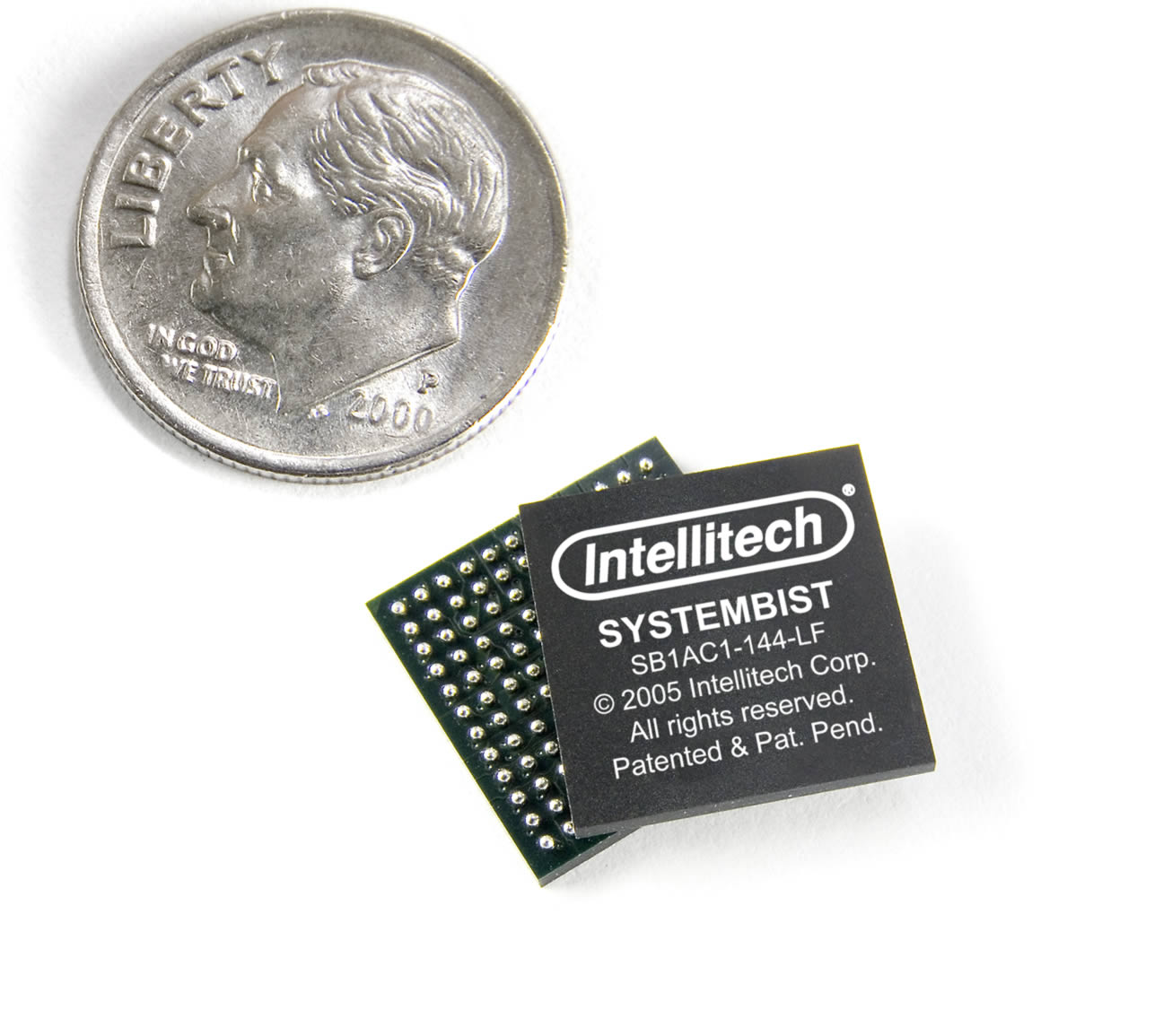
SystemBIST - The programmable configuration device with JTAG control
SystemBIST
uses a PC based software application and GUI enabling you to develop
complex FPGA configuration methods, control of I2C/SPI devices and add
in-system JTAG based manufacturing tests.
The software application creates a single image of your FPGA data,
test data and flow-control sequences which is then downloaded to the on-PCB
SystemBIST and memory. Updates are
done by examining the differences in data, creating an incremental image
and erasing/programming a safe portion of the memory.
It’s not just an IC, but a whole ecosystem of software,
companion ICs, downloadable IP and support services integrated to get many
engineering tasks done on time and at the lowest cost. This ecosystem
creates a stable, high performance re-usable solution that frees the
engineers to focus on product development rather than reinventing
board-level infrastructure. Use SystemBIST and reduce development costs,
test engineering costs, parts costs, field service costs, schedule and
logistic risks and time-to-deployment.
|
|
|
|
|
Feature
|
Benefit
|
- IC and software
is integrated for 'fail-safe' in-the-field FPGA updates
|
Easy to use
FPGA/CPLD updating in the field
|
- Load multiple
designs into each FPGA based on PCB configuration, geographical
location, FPGAs present, DSP algorithms needed, Telecom standards
needed or other user definable conditions
|
Greater than 100%
FPGA device utilization
|
- Execute JTAG
based manufacturing tests embedded with FPGA data
|
Pinpoint defects
and opens without ATE. Provides
critical data point on low-level hardware status reducing debug
time. Execute tests over operating
environment, during burn-in and at customer site, load test specific FPGA
designs
|
- Test/FPGA
configuration results saved in non-volatile memory
|
Eliminates NTF returns,
enables high resolution defect identification by SystemBIST application
software – even for PCBs in-the-field
|
- Load IJTAG
tests for SERDES and DDR memories
|
Enables at-speed
infrastructure tests with pinpoint diagnostics
|
- Programmable PCB
level resets
|
Control bring up
of CPUs and FPGA
|
|
|
Control DC/DC converters, LEDs, control I2C/SPI A/D or D/A
|
|
|
Reset CPU or FPGAs
on ‘hang’ , reduce component count
|
|
|
|
|
|
|
|
|
|
|
 DesignCon Booth 124, Santa Clara Convention
Center , February 5-6th DesignCon Booth 124, Santa Clara Convention
Center , February 5-6th
|